
This article is part of the Technology Insight series, made possible with funding from Intel.
As we create more content, deploy more sensors at the network’s edge, and replicate more data for AI to contextualize, the demand for compute bandwidth roughly doubles every three years. Keeping up is becoming increasingly difficult as modern computing architectures get closer and closer to the theoretical performance limits of electrical connections linking their processors, storage, and networking components.
Silicon photonics technology—a combination of silicon integrated circuits and semiconductor lasers—may help overcome the bottlenecks imposed by electrical I/O, replacing copper connections with optical ones at the board and package level.
According to James Jaussi, senior principal engineer and director of Intel’s PHY research lab, miniaturized silicon photonics components open the door to architectures that are more disaggregated. That could look like pools of compute, memory, and peripheral functionality distributed throughout the system; connected over long distances with optical links, software-defined infrastructure, and high-speed networking.
For now, integrated photonics is still the stuff of lab experiments. But a number of breakthroughs introduced during Intel’s recent Labs Day show that the technology is capable of lower power, higher performance, and greater reach than today’s server interconnects.
KEY POINTS:
- Silicon photonics technology is already bringing down costs and improving availability of high-speed optical transceivers.
- The miniaturization of silicon photonics components opens the door to board-to-board and package-to-package optical I/O.
- Recent research promises to overcome impending performance and power scaling issues facing electrical I/O.
Silicon photonics is already pervasive in the datacenter
Today, silicon photonics technology is used in datacenters for connecting switches that might be miles apart. On one end, transceivers (devices able to transmit and receive) convert electrical signals to light, which is then sent across optical fiber. At the other end, those optical signals are changed back into electrical. What makes the conversion from electrical to optical a worthwhile endeavor? In short, higher bandwidth, coverage over greater distances, and an immunity to electromagnetic interference.
But traditional optical transceivers are expensive. Their transmitter and receiver sub-assemblies must be carefully constructed and hermetically sealed for protection, which makes it difficult for manufacturers to keep up with demand. And the myriad of components that go into a transceiver take up significant space.
Silicon photonics packs many of the optical and electronic pieces used to build a transceiver into highly integrated chips. These chips are manufactured in advanced fabs by the same machines that produce the latest CPUs, GPUs, and FPGAs. They enjoy the benefits of cutting-edge lithography, automation, and economies of scale, making them much smaller and less expensive than the technology they replace.
Intel introduced its own family of 100 Gb/s transceivers based on semiconductor lasers back in 2016, ten years after demonstrating the technology alongside researchers from UC Santa Barbara. It quickly scored wins with performance-sensitive customers like Microsoft’s Azure cloud computing service. Since then, it has shipped more than four million 100 Gb/s modules, according to Labs Day presentations.
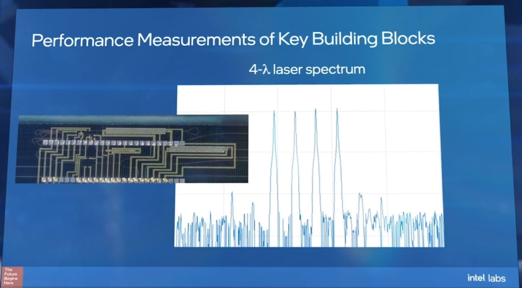
Above: Intel’s hybrid silicon laser generates light at four wavelengths from a single laser cavity.
Image Credit: Intel
Intel has its sights set on scaling optical I/O volumes several orders of magnitude higher though—into the billions of devices. That would take optical beyond rack-to-rack communications in the datacenter and down to the board level, right onto the compute engines where electrical I/O currently dominates. Intel calls this research integrated photonics.
Miniaturized silicon photonics as an electrical interconnect alternative
If electrical I/O works so well between the server boards and processing packages, why look to silicon photonics as a replacement? Unfortunately, electrical interconnects are struggling to keep those resources fed, and every bit of speed-up comes at the cost of disproportionately more power consumption. There’s a wall in sight, and that’s making optical I/O an appealing alternative.
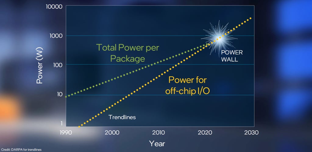
Above: Over time, the power requirements of electrical I/O are trending larger than the total available socket power, leaving nothing for compute engines.
Image Credit: Intel
Although silicon photonics transceivers offer notable advantages over traditional optical designs, their components are still too large, too expensive, and too power-hungry to displace electrical I/O within servers. The breakthroughs announced at Labs Day 2020 change this.
Jaussi says there are six ingredients in the company’s recipe for integrated photonics: light generation, amplification, detection, modulation, CMOS interface circuits, and package integration. Intel already has a hybrid silicon laser in its portfolio, which is used on its silicon photonics transceivers for converting electrical signals into light. So, it’s focusing on the other five building blocks.
What will it take to enable integrated photonics on compute packages?
In a basic transmitter, the laser creates light onto which data is encoded by a modulator. Existing silicon modulators are large, and therefore expensive in the context of integrated photonics. New micro-ring modulators announced during Labs Day shrink this component’s footprint by more than 1000x. Voltage supplied by a circuit above the modulator either traps light in the ring or allows it to travel down its waveguide.
A detector at the other end interprets the absence or presence of light as zeroes and ones. The photodiodes in existing silicon photonics optical transceivers rely on materials like Germanium or Indium Phosphide to “see” light in the wavelengths used to move data. Silicon, it was thought, had no light detection capability in that range. Intel showed otherwise by using its all-silicon micro-ring structure as a photodetector operating at 112 Gb/s. “A major advantage of this development is processing and material cost reduction,” says Jaussi.
Intel multiplies the bandwidth through each fiber by capturing multiple wavelengths (or colors) of light from one laser. This technology is called wavelength division multiplexing. In his Labs Day demo, Jaussi showed four micro-rings trapping four separate wavelengths from a single optical channel to convey four bits of data. In the early days of silicon photonics research, this would have taken four different lasers, plus a multiplexer. Doing it with one is key to moving data fast enough in a space-constrained application like on-package I/O, where there isn’t room for lots of laser firing next to each other.
The addition of a semiconductor optical amplifier helps optimize integrated photonics systems for power consumption, since an amplifier provides light power more efficiently than the laser. These amplifiers are made from the same materials as the multi-wavelength laser—an important consideration for manufacturing at volume.
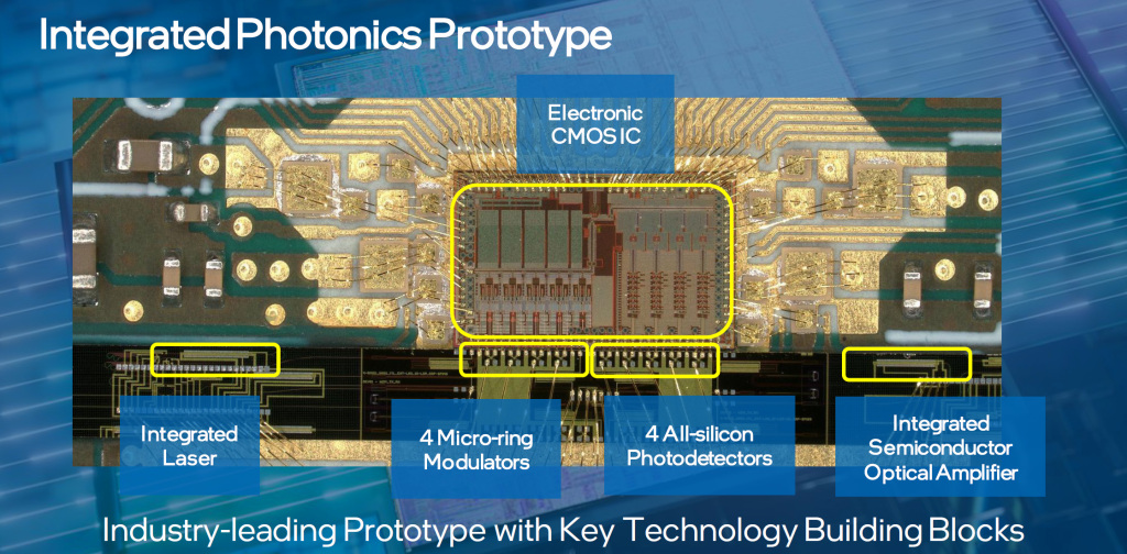
Above: Intel’s integrated photonics prototype features an electronic CMOS IC stacked on top of a photonics IC in a 3D package, combining the benefits of silicon integrated circuits and semiconductor lasers.
Image Credit: Intel
Combining cutting-edge photonics and cost-effective fabrication
As part of Intel’s Labs Day demonstration, Haisheng Rong, principal engineer at Intel Labs, showed off a photonic IC with the hybrid silicon laser, micro-ring modulators, an optical amplifier, and micro-ring photodetectors integrated together and manufactured in a high-volume CMOS fab. He was joined by fellow principal engineer Ganesh Balamurugan, who described the electrical IC responsible for driving and controlling Intel’s micro-ring modulators. The two ICs are stacked, one on top of the other, and connected with copper pillars.
“This is an example of how we can tightly integrate energy-efficient CMOS circuits with silicon photonics using 3D packaging,” says Balamurugan. “Such cointegration is key to delivering performance and cost-optimized optical transceivers.”
By integrating silicon photonics building blocks with compute resources, Intel believes it can break the current trend of larger processors with more I/O pins, which are needed to satisfy growing bandwidth requirements. Silicon photonics makes it possible to achieve lower power consumption, greater throughput between compute elements, and reduced pin counts, all in a smaller footprint.
Above: Back in March 2020, Intel announced the successful integration of its 1.6 Tb/s silicon photonics engine with its 12.8 Tb/s programmable Ethernet switch, putting optical I/O on the same package as a Barefoot Tofino 2 ASIC for the first time.
Image Credit: Intel
The company is already showing off high-performance Ethernet switch silicon co-packaged with silicon photonics engines, designed to address the power and cost/complexity issues posed by electrical I/O scaling limitations within two switch generations.
It’ll be longer before we see integrated photonics inside of servers—Intel acknowledges that the technology isn’t on the product implementation path yet. However, over time, the company hopes to scale its silicon photonics platform up to 1 Tb/s per fiber at 1pJ of energy consumed per bit, reaching distances of up to 1 km. With electrical I/O facing an impending power wall and silicon photonics already a successful component of Intel’s networking catalog, this is a technology you’ll want to keep an eye on.